- 您现在的位置:买卖IC网 > Sheet目录3841 > PIC16C63A-04I/SO (Microchip Technology)IC MCU OTP 4KX14 PWM 28SOIC
107
SAM7S Series [DATASHEET]
6175M–ATARM–26-Oct-12
19.2.2
Read Operations
An optimized controller manages embedded Flash reads. A system of 2 x 32-bit buffers is added in order to start
access at following address during the second read, thus increasing performance when the processor is running in
This optimization concerns only Code Fetch and not Data.
The read operations can be performed with or without wait state. Up to 3 wait states can be programmed in the
field FWS (Flash Wait State) in the Flash Mode Register MC_FMR (see “MC Flash Mode Register” on page 115).
Defining FWS to be 0 enables the single-cycle access of the embedded Flash.
The Flash memory is accessible through 8-, 16- and 32-bit reads.
As the Flash block size is smaller than the address space reserved for the internal memory area, the embedded
Flash wraps around the address space and appears to be repeated within it.
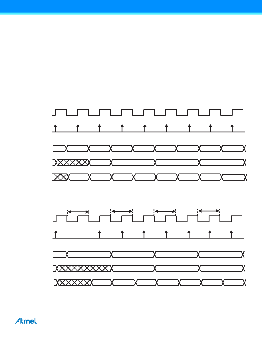
Figure 19-2. Code Read Optimization in Thumb Mode for FWS = 0
Note:
When FWS is equal to 0, all accesses are performed in a single-cycle access.
Figure 19-3. Code Read Optimization in Thumb Mode for FWS = 1
Note:
When FWS is equal to 1, in case of sequential reads, all the accesses are performed in a single-cycle access (except for the
first one).
Flash Access
Buffer (32 bits)
Master Clock
ARM Request (16-bit)
Code Fetch
Data To ARM
Bytes 0-3
Bytes 4-7
Bytes 0-3
Bytes 0-1
Bytes 2-3
Bytes 4-5
Bytes 6-7
Bytes 8-9
Bytes 10-11
Bytes 12-13
@Byte 0
@Byte 2
@Byte 4
@Byte 6
@Byte 8
@Byte 10
@Byte 12
@Byte 14
@Byte 16
Bytes 14-15
Bytes 4-7
Bytes 8-11
Bytes 12-15
Bytes 16-19
Bytes 12-15
Flash Access
Buffer (32 bits)
Master Clock
ARM Request (16-bit)
Code Fetch
Data To ARM
Bytes 0-3
Bytes 4-7
Bytes 0-3
Bytes 2-3
Bytes 4-5
Bytes 6-7
Bytes 8-9
Bytes 10-11
@Byte 0
@Byte 4
@Byte 6
@Byte 8
@Byte 10
@Byte 12
@Byte 14
Bytes 4-7
Bytes 8-11
Bytes 12-15
1 Wait State Cycle
Bytes 0-1
1 Wait State Cycle
@Byte 2
Bytes 12-13
发布紧急采购,3分钟左右您将得到回复。
相关PDF资料
52559-2270
CONN FFC 22POS .5MM VERT ZIF SMD
52559-1870
CONN FFC 18POS .5MM VERT ZIF SMD
DSPIC33EP64MC506-I/PT
IC DSC 16BIT 64KB FLASH 64TQFP
52745-1896
CONN FFC 18POS .5MM R/A ZIF SMD
PIC16LC622-04/P
IC MCU OTP 2KX14 COMP 18DIP
PIC16LF84A-04/P
IC MCU FLASH 1KX14 EE 18DIP
DSPIC30F1010-30I/MM
IC DSPIC MCU/DSP 6K 28QFN
52745-1696
CONN FFC 16POS .5MM R/A ZIF SMD
相关代理商/技术参数
PIC16C63A-04I/SP
功能描述:8位微控制器 -MCU 7KB 192 RAM 22 I/O RoHS:否 制造商:Silicon Labs 核心:8051 处理器系列:C8051F39x 数据总线宽度:8 bit 最大时钟频率:50 MHz 程序存储器大小:16 KB 数据 RAM 大小:1 KB 片上 ADC:Yes 工作电源电压:1.8 V to 3.6 V 工作温度范围:- 40 C to + 105 C 封装 / 箱体:QFN-20 安装风格:SMD/SMT
PIC16C63A-04I/SS
功能描述:8位微控制器 -MCU 7KB 192 RAM 22 I/O RoHS:否 制造商:Silicon Labs 核心:8051 处理器系列:C8051F39x 数据总线宽度:8 bit 最大时钟频率:50 MHz 程序存储器大小:16 KB 数据 RAM 大小:1 KB 片上 ADC:Yes 工作电源电压:1.8 V to 3.6 V 工作温度范围:- 40 C to + 105 C 封装 / 箱体:QFN-20 安装风格:SMD/SMT
PIC16C63A04SP
制造商:MICROCHIP 功能描述:NEW
PIC16C63A-20/SO
功能描述:8位微控制器 -MCU 7KB 192 RAM 22 I/O RoHS:否 制造商:Silicon Labs 核心:8051 处理器系列:C8051F39x 数据总线宽度:8 bit 最大时钟频率:50 MHz 程序存储器大小:16 KB 数据 RAM 大小:1 KB 片上 ADC:Yes 工作电源电压:1.8 V to 3.6 V 工作温度范围:- 40 C to + 105 C 封装 / 箱体:QFN-20 安装风格:SMD/SMT
PIC16C63A-20/SP
功能描述:8位微控制器 -MCU 7KB 192 RAM 22 I/O RoHS:否 制造商:Silicon Labs 核心:8051 处理器系列:C8051F39x 数据总线宽度:8 bit 最大时钟频率:50 MHz 程序存储器大小:16 KB 数据 RAM 大小:1 KB 片上 ADC:Yes 工作电源电压:1.8 V to 3.6 V 工作温度范围:- 40 C to + 105 C 封装 / 箱体:QFN-20 安装风格:SMD/SMT
PIC16C63A-20/SP
制造商:Microchip Technology Inc 功能描述:8 Bit Microcontroller Clock Speed:20MHz
PIC16C63A-20/SS
功能描述:8位微控制器 -MCU 7KB 192 RAM 22 I/O RoHS:否 制造商:Silicon Labs 核心:8051 处理器系列:C8051F39x 数据总线宽度:8 bit 最大时钟频率:50 MHz 程序存储器大小:16 KB 数据 RAM 大小:1 KB 片上 ADC:Yes 工作电源电压:1.8 V to 3.6 V 工作温度范围:- 40 C to + 105 C 封装 / 箱体:QFN-20 安装风格:SMD/SMT
PIC16C63A-20E/SO
功能描述:8位微控制器 -MCU 7KB 192 RAM 22 I/O RoHS:否 制造商:Silicon Labs 核心:8051 处理器系列:C8051F39x 数据总线宽度:8 bit 最大时钟频率:50 MHz 程序存储器大小:16 KB 数据 RAM 大小:1 KB 片上 ADC:Yes 工作电源电压:1.8 V to 3.6 V 工作温度范围:- 40 C to + 105 C 封装 / 箱体:QFN-20 安装风格:SMD/SMT